600- and 700-volt super junction MOSFETs with high power density
2022-03-04
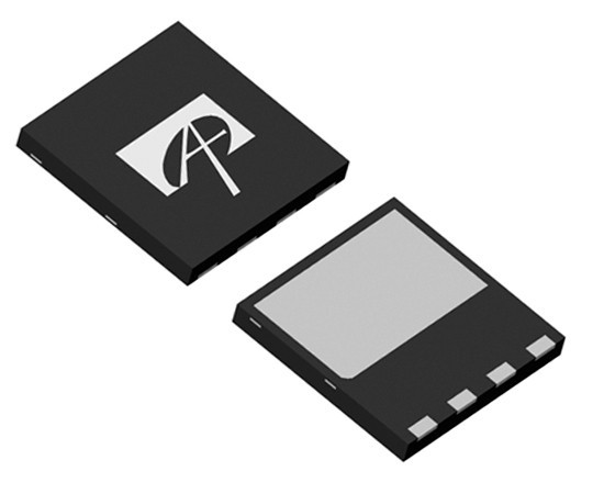
The αMOS5 transistors in 8x8 DFN housings feature a nearly 60% smaller footprint than the D2Pak standard, and their thickness, at 0. 9 mm, is 80% less.
Reduced source inductance provides less oscillation at the gate and less turn-on loss (Eon). The Kelvin lead-out on the transistor source further reduces losses during pulse operation. ΑMOS5 transistors encapsulated in 5x6 DFN enclosures occupy 61% less area than transistors in DPak enclosures. They are only 0. 75 mm thick, 67% less than the thickness of DPAK enclosures. As with the DFN 8x8 version, these transistors have the advantage of low source inductance, allowing applications in fast pulse circuits.
| SYMBOL | DESCRIPTION |
|---|---|
|
|
600V, A MOS5 TM N-CHANNEL POWER |
|
|
700V, A MOS5 TM N-CHANNEL POWER |
|
|
700V, A MOS TM N-CHANNEL POWER T |